Star Wars Troubleshooting Guide |
 |
You will definitely need a "table capable" browser for this page
Troubleshooting With the Diagnostics Program
Troubleshooting With the CAT Box
Introduction
The STAR WARS game circuitry is contained on three printed-circuit boards (PCB): the Analog Vector-Generator (AVG) PCB, the Main PCB, and the Sound PCB.
The AVG PCB contains the analog vector-generator which draws the lines on the screen. It has 12 kilobytes of vector RAM and 4 kilobytes of vector ROM.
The Main PCB contains the 68B09E game microprocessor; 48 kilobytes of program ROM; 2 kilobytes of program RAM; option switches; means for reading control panel switches and potentiometers; a pseudo-random number generator; a digital divider; and a matrix processor which performs the math for the three dimensional graphics.
The Sound PCB contains a 68B09E microprocessor; 16 kilobytes of ROM (for the program, sound tables, and speech vocabulary); a 6532A peripheral interface adapter (with 128 bytes of RAM, two bidirectional input/output (I/O) ports, and an interrupt timer); 2 kilobytes of RAM; a speech synthesizer; four custom music and sound effects generators; a stereo image synthesizer; and an interface to the Main PCB.
The Self-Test Mode (selected by the Self-Test switch on the utility panel) tests most of the hardware. Refer to Chapter 2 of the Operators Manual for the basic self-test procedures. This game also includes a Hardware Diagnostic Mode, which permits the repair technician to select specific hardware diagnostic tests to aid in troubleshooting (refer to Hardware Diagnostic Tests for additional information). This Troubleshooting Guide describes the recommended method for effectively using the Self-Test and Hardware Diagnostic Tests to quickly locate defective components.
Carefully read the following Trouble Analysis discussion before attempting to perform the troubleshooting procedures.
Trouble Analysis
A thorough analysis of the trouble symptoms with the aid of the following discussion, should help to quickly localize the trouble to a major circuit.
Preliminary Procedure
- Perform the Self-Test Procedure as described in Chapter 2 of the Operators Manual. If the self-test is not helpful, or is inoperative, proceed with part 2.
- Check the power supply voltages and the clocks.
- NOTE - The Sound PCB can be tested without the Main and AVG PCB completely working.
- Perform Hardware Diagnostic Test 1 to determine if enough of the Main PCB memory is functioning to perform additional tests.
- Perform Hardware Diagnostic Test 2 to determine if the AVG PCB memory is faulty. The vector generator may not work if its memory is faulty.
- If the AVG memory is functioning properly, but the remaining AVG circuitry is not, perform Hardware Diagnostic Tests 3 through 8. The AVG circuitry must be functioning properly before proceeding to part 6.
- If parts 2 through 5 have been performed, enough of the system should be working so that the Self-Test Procedure can be accomplished as described in Chapter 2 of the Operators Manual. If there are problems in the divider or matrix processor, the Mathbox Tests display will indicate which tests failed and the number of the appropriate Hardware Diagnostic Test for troubleshooting the faulty circuit. If there are problems in the RAM or ROM on the Main or AVG PCB, the Hardware Errors display will indicate which RAM or ROM is faulty by the characteristics of the tones that accompany the Hardware Errors display. The following procedure describes the method for performing a self-test of the program and analog vector-generator RAM and ROM.
Program and Analog Vector-Generator RAM/ROM Self-Test
 Check the condition of the RAM and ROM on the Main and AVG PCB as follows:
- Obtain the Hardware Errors display as described in Chapter 2 of the Operators Manual.
- Immediately after the Hardware Errors display appears, a series of 16 tones should be heard that indicates the condition of the program RAM and analogvector generator. The series of tones, separated by a short pause, will repeat indefinitely. A high upwardsweeping tone indicates a properly operating RAM or ROM, while a low downward-sweeping tone indicates a faulty RAM or ROM. Count the tones to determine the location of the faulty RAM or ROM as shown in Table 1.
If the preceding RAM and ROM self-test did not locate the problem, refer to the following symptoms for additional trouble-analysis information:
- No sound, but video is present and the game seems to work. Check the Sound PCB, Regulator/Audio II PCB, or the speakers.
- NOTE - The volume control on the utility panel is wired to the input of the power amplifiers (rather than the output) so that the amplifiers will run at full volume if the utility panel is disconnected.
- No video, but there is sound and the game seems to work. Check the AVG PCB or the display. If the display is suspect, substitute a known good display or use an X-Y oscilloscope connected to the AVG X and Y outputs to troubleshoot the display. If an X-Y oscilloscope is not available, use the normal sweep mode and check at the X, Y, R, G and B test points. In either case, verify that the X, Y. R. G. and B outputs are present. If problems still exist, refer to Troubleshooting the AVG PCB.
- Some video, but no enemy ships or stars. Check the matrix processor and divider circuits by obtaining the Mathbox Tests display with the game in the SelfTest Mode as described in Chapter 2 of the Operators Manual. If the BAD MATH READY LINE message appears and the math ready line is stuck low, the result will be some video. but no enemy ships or stars. If the BAD MATH READY LINE message appears and the math ready line is stuck high, the screen will be completely blank in game mode (but will function during Self-Test).
- Everything seems to work, but there are no stars in the space wave, and all the dots on the ground in the Tower wave come from the same point. Check the pseudo-random number generator at locations 4D, 5B, 5C, and 5D on the Main PCB. Make sure the 3-MHz clock is present and that PRNGCLR is not permanently low. PRNGCLR is made low by a hardware reset and made high by the microprocessor. If the program is not running, the pseudo random number generator will remain cleared. If the pseudorandom number generator is working, connect a 2.2-kilohm resistor from pin 13 of the integrated circuit at location 5D to pin 1 of connector J16 and listen for white noise.
- CAUTION - Switch 8 on the option switch at location 10D on the Main PCB selects a freeze mode. By pressing the left fire trigger on the flight control, the display can be advanced frame-by-frame. Some frames use an extra-high brightness level to achieve special effects, e.g., the Death Star explosion. During normal game play, these effects last for a short time; thus, there is no danger to the CRT or the display circuitry. However, if these frames are displayed for too long in the freeze mode, the CRT screen could be burned and/or the display circuitry damaged.
Troubleshooting the Sound PCB
The following procedure is recommended if the game is completely inoperative and it has been determined that the problem is not a faulty display. The Sound PCB can be tested without the Main PCB or AVG PCB fully operative. The Main PCB must be connected, although the AVG PCB can be removed for this procedure.
- Visually inspect the Sound PCB for obvious problems:
- Loose, missing, or improperly oriented integrated circuits.
- Solder shorts.
- Check for the following voltages:
- Check for the following clocks:
- CLK E (1.5 MHz)
- CLK Q (1.5 MHz in quadrature with CLK E)
- 6 MHz
- Check that the RESET line to the microprocessor at location 2C on the Main PCB is normally high and goes low when the RESET test point on the Main PCB is momentarily grounded. If necessary, ground the WDDIS and HALT test points on the Main PCB.
- Check that the IRQ line to the Sound PCB microprocessor at location 3K is not permanently low. It is acceptable if the IRQ line is intermittently low; but, a permanent low indicates a fault that could be caused by a trace short, a defective peripheral interface adapter at location 1E, or the program not running.
- NOTE - If the above signals, voltages, and clocks are present, the following self-test procedures can be performed on the Sound PCB even if everything else on the Main PCB and AVG PCB is inoperative.
RAM and ROM Test

- Set the Self-Test switch to the on (up) position (unless the WDDIS and the HALT test points on the Main PCB have been grounded).
- Ground the SELF-TEST test point on the Sound PCB (ignore the sounds) and then momentarily ground the RESET test point on the Main PCB.
- Verify that a series of four tones is heard after the RESET test point is grounded. The series of tones, separated by a short pause, will be repeated indefinitely. A high tone indicates a good RAM or ROM; a low tone indicates a faulty RAM or ROM. Count the tones and use Table 2 to locate a faulty RAM or ROM on the Sound PCB.
- Unground the SELF-TEST test point on the Sound PCB.
Music and Sound Effects Generators Test
- Set the Self-Test switch to the on (up) position.
- Obtain the Switch Test self-test display as described in Chapter 2 of the Operators Manual.
- Ground the SELF-TEST test point on the Sound PCB until the first sound is heard, then remove the ground.
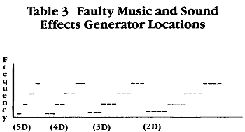
- A series of four long tones (one for each channel or voice) should be heard with each succeeding tone rising in frequency which indicates that Cl/O 0 at location 5D is good. After a very short pause, a set of four double tones should occur, which indicates that Cl/O 1 at location 4D is good. See Table 3 for a graphic representation of the tones and the location of the music and sound effects generator from which they originate.
- Again, ground the SELF-TEST test point until a set of four triplet tones is heard, which indicates that CI/O 2 at location 3D is good. The last set of four quadruplet tones indicates that CI/O 3 at location 2D is good. See Table 3 for a graphic representation of the tones and the location of the music and sound effects generator from which they originate.
- Ground the SELF-TEST test point on the Sound PCB. A sound should be heard after a short interval. With the SELF-TEST test point continuously grounded, a series of two-second sound segments comprising three sound groups (voice, music, and sound effects) should be heard. By ungrounding the SELF-TEST test point as soon as a sound segment starts, that particular sound should finish regardless of its duration. Ground the SELF-TEST test point again to continue with the next sound segment.
- Repeat the preceding tests by momentarily grounding the RESET test point on the Main PCB and performing parts 2 through 6.
If there is no audible sound for any of the preceding tests, connect an oscilloscope to pin 8 of the speech synthesizer at location lC/D on the Sound PCB and look for some obvious activity when the speech test is supposed to be running (about 10 seconds after the RESET test point on the Main PCB is grounded). Repeat this procedure at the outputs of the music and sound effects generators buffers located on the Sound PCB (4C-pin 1, 4C-pin 7, 3C-pin 1, and 3C-pin 7). Even when the music and sound effects generators are working, there will be no measurable signals at the outputs of the custom sound integrated circuits themselves because the buffers act as currentsumming amplifiers.
If the oscilloscope indicates that audio is present but there is no audible sound, trace the signal downstream to the speakers. If problems still exist, refer to Troubleshooting With the CAT Box for the procedure on Troubleshooting the Sound PCB.
Troubleshooting the Main and AVG PCB
If the AVG PCB was removed while testing the Sound PCB, it should be reinstalled for the following tests (the Sound PCB can be removed for this test). If the HALT test point on the Main PCB was grounded for the Sound PCB test, remove the ground jumper.
If the Main and AVG PCB circuits are both faulty, first check the Main PCB as follows:
- Visually inspect the board for obvious problems:
- Loose, missing, or improperly oriented integrated circuits.
- Solder shorts.
- Check for the following voltages:
- + 5 V
- + 12 V
- + 5 V EAROM (there is a separate + 5 V for the nonvolatile RAM)
- + 10.3 V unregulated.
- Check for the following clocks:
- 12 MHz
- 6 MHz
- 3 MHz
- 1.5 MHz
- E
- Q
- Check that the microprocessor HALT, NMI, and FIRQ lines are always high.
- Check that the microprocessor RESET line is high except when the RESET test point is grounded. If necessary, disable the watchdog circuit by grounding the WDDIS test point on the Main PCB. Refer to Troubleshooting the Watchdog Circuit if the watchdog circuit is not working.
- Check that the microprocessor IRQ line is not permanently low. (An intermittent low on the IRQ line is acceptable.)
- Perform Hardware Diagnostic Test 1 to check that the Main PCB RAM and ROM is working. If the RAM or ROM is faulty, refer to Troubleshooting With the CAT Box for checking the Main PCB.
If the Main PCB RAM or ROM is working and there is no display, check the AVG PCB as follows:
- Visually inspect the AVG PCB for obvious problems:
- Loose, missing, or improperly oriented integrated circuits.
- Solder shorts.
- Check for the following voltages:
- + 5 VDC
- + 12 VDC
- + 15 VDC
- + 22 VDC
- - 22 VDC
- - 15 VDC
- Check for the following clocks:
- 12 MHz
- 6 MHz
- 3 MHz
- VGCLK (1.5 MHz)
If the voltages and clocks are present, perform Hardware Diagnostic Test 2 to determine if the vector generator RAM and ROM are working.
If the vector generator RAM and ROM are working, but the vector generator is faulty, perform Hardware Diagnostic Test 3 through 8. These tests will enable you to trace the micro-operation of each vector-generator instruction.
Another method of determining a vector generator hardware failure is to use signature analysis, which is selected by Hardware Diagnostic Test 9. (See Analog VectorGenerator Signature Analysis).
Troubleshooting the Watchdog Circuit
The watchdog circuit will send continuous reset pulses to the microprocessor on the Main PCB if a problem exists in the microprocessor circuit. If the Self-Test Mode is inop-
erative, check the RESET line. RESET is a microprocessor input (pin 37). Normally, reset should occur during powerup or when the RESET test point is grounded. A pulsing RESET line indicates that something is causing the microprocessor to lose its place in the program. Typical causes are:
- Open or shorted address or data bus lines.
- Faulty microprocessor.
- Faulty bus buffers.
- Faulty RAM or ROM.
- Any faulty input or output that causes an address or data line to be held in a constant high or low state.
- NOTE - To aid in troubleshooting, connect the WDDIS test point to ground to prevent resets.
Hardware Diagnostic Tests
The Hardware Diagnostic Tests use the option switches at location 10D on the Main PCB. (Remember to restore the option switches to their proper setting when the diagnostic testing is completed.)
Preliminary Procedure
- Set the Self-Test switch to the on (up) position.
- Ground the DIAGN test point on the Main PCB.
- Set the option switches as indicated in the test procedure and momentarily ground the RESET test point on the Main PCB. If an unimplemented switch position is selected, LED 1, 2, and 3 on the Main PCB will all flash on and off about once per second. Also, the display will show the number of the test for Hardware Diagnostic Tests 10 through 26 (if the AVG PCB and display are working).
- Consider the following suggestions:
- If a significant number of tests are to be performed attach a small momentary on, normally off, pushbutton switch to the RESET test points.
- Remove the high-score and bookkeeping nonvolatile RAM (NOVRAM) from location 1E on the Main PCB while troubleshooting the rest of the hardware. Each time the RESET test point is grounded, one of the RAM store cycles is used up. The nonvolatile RAM is rated for either 10,000 store cycles if the data is not changed, and 1,000 store cycles if the data is changed.
Main PCB Microprocessor and Memory Test
The following test determines whether the 68B09E microprocessor, ROM 4, and program RAM on the Main PCB are working together to enable the basic Self-Test and Hardware Diagnostic Tests to be performed.
Test 1
- Perform the Preliminary Procedure under Hardware Diagnostic Tests.
- Set the option switch at location 10D on the Main PCB as follows:
| 8 | 7 | 6 | 5 | 4 | 3 | 2 | 1 |
| OFF | OFF | OFF | OFF | OFF | OFF | OFF | OFF |
- NOTE - If Test 2 was performed just prior to Test 1, omit part 3 and proceed to part 4.
- Momentarily ground the RESET test point on the Main PCB. LED 1, 2, and 3 should all light and remain lit for about 10 seconds.
- If the microprocessor is running, LED 2 and 3 will extinguish and LED 1 will flash on and off about once per second. LED 2 and 3 must be off; if not, the microprocessor may be running in a failure mode with the RAM and ROM not working.
LED 1 will be set to flash (or not flash) depending on the results of the test, and will continue in that state until another test is selected or the RESET test point is grounded. For example, if something happens after the test that either corrects the faulty program RAM or causes a malfunction, the diagnostic program will not recognize it and LED 1 will continue to flash (or not flash) until the RESET test point is grounded to repeat the test again.
- If the microprocessor is not running, disconnect the Sound PCB or the AVG PCB. If the microprocessor begins to work, the problem may be a short on one of the address or clock lines on the Sound or AVG PCB.
- If the problem still exists, refer to Troubleshooting With the CAT Box for checking the Sound and AVG PCB.
Analog Vector-Generator Memory Test
This test determines the condition of the vector generator RAM and ROM on the AVG PCB.
Test 2
- Perform the Preliminary Procedure under Hardware Diagnostic Tests.
- Set the option switch at location 10D on the Main PCB as follows:
| 8 | 7 | 6 | 5 | 4 | 3 | 2 | 1 |
| ON | OFF | OFF | OFF | OFF | OFF | OFF | OFF |
- NOTE - If Test 1 was performed just prior to Test 2, omit part 3 and proceed to part 4. If Test 1 or 2 is selected after other tests have been selected, the RESET switch must be pressed again to perform the test.
- Momentarily ground the RESET test point on the Main PCB. LED 1, 2, and 3 should all light and remain lit for about 10 seconds.
- LED 1 and 3 will extinguish, and, if the vector generator RAM and ROM are working, LED 2 will flash on and off about once per second.
LED 2 will be set to flash (or not flash) depending on the results of the test and will continue in that state until another test is selected or the RESET test point is grounded. For example, if something happens after the test that either corrects the faulty vector generator RAM or ROM or causes a malfunction, the diagnostic program will not recognize it and LED 2 will continue to flash (or not flash) until the RESET test point is grounded to repeat the test again. (The memory portion of Test 1 and 2 are accomplished simultaneously.)
Analog Vector-Generator Instructions Tests
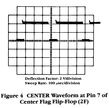
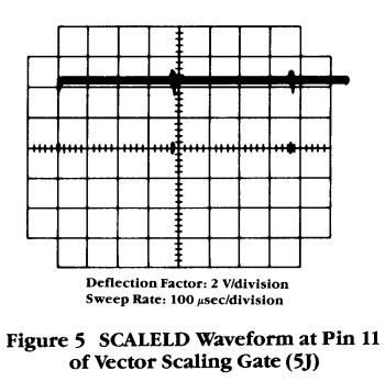
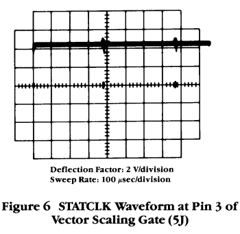
The following Test 3 through 9 generate specific analog vector-generator instructions. Each test is retriggered every 400 microseconds for as long as the test is selected. The appropriate waveform obtained at each test point is included for each test.
Perform the Preliminary Procedure under Hardware Diagnostic Tests and set the option switch at location 10D on the Main PCB as indicated for each test.
- NOTE - It is not necessary to ground the RESET test point on the Main PCB when selecting within the following Test 3 through 9. Also, if the Atari PAT 9000 Programmable Test Station is used, turn off the color X-Y monitor.
Test 3
Option Switch Settings:
| 8 | 7 | 6 | 5 | 4 | 3 | 2 | 1 | | ON | ON | OFF | OFF | OFF | OFF | OFF | OFF | |
 |
Test 4
Option Switch Settings:
| 8 | 7 | 6 | 5 | 4 | 3 | 2 | 1 | | ON | ON | OFF | OFF | OFF | OFF | OFF | ON | |
 |
Test 5
Option Switch Settings:
| 8 | 7 | 6 | 5 | 4 | 3 | 2 | 1 | | ON | ON | OFF | OFF | OFF | OFF | ON | OFF | |
 |
Test 6
Option Switch Settings:
| 8 | 7 | 6 | 5 | 4 | 3 | 2 | 1 | | ON | ON | OFF | OFF | OFF | OFF | ON | ON | |
 |
Test 7
Option Switch Settings:
| 8 | 7 | 6 | 5 | 4 | 3 | 2 | 1 | | ON | ON | OFF | OFF | OFF | ON | OFF | OFF | |
 |
Test 8
Option Switch Settings:
| 8 | 7 | 6 | 5 | 4 | 3 | 2 | 1 | | ON | ON | OFF | OFF | OFF | ON | OFF | ON | |
 |
Test 9
Option Switch Setting:
| 8 | 7 | 6 | 5 | 4 | 3 | 2 | 1 | | ON | ON | OFF | OFF | OFF | ON | ON | OFF |
| |
This test is for Analog Vector-Generator signature analysis. See Analog Vector-Generator Signature Analysis procedure. |
Matrix Processor Instructions Tests
The following Test 10 through 20 generates specific matrix processor instructions. The correct hexadecimal address for bits zero through nine on the matrix processor address bus are included for each test. The test number will be shown on the display (assuming that the display and AVG PCB are working). Each test is retriggered every 28 to 84 microseconds for as long as the test is selected.
Perform the Preliminary Procedure under Hardware Diagnostic Tests and set the option switches at location 10D on the Main PCB as indicated in the test.
- NOTE - It is not necessary to ground the RESET test point on the Main PCB when selecting within the following Test 10 through 20.
Test 10
 Option Switch Setting:
| 8 | 7 | 6 | 5 | 4 | 3 | 2 | 1 |
| ON | ON | ON | OFF | OFF | OFF | OFF | OFF |
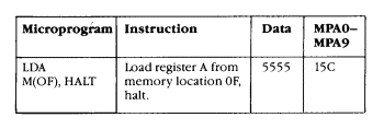
Test 10 performs the following operations:
- The 68B09E microprocessor on the Main PCB writes a 15C into the matrix processor address counter during MWO which forms the address for the instruction PROM and is the starting address of the microprogram to be executed. MWO also sets the flip-flop at location 8H in the matrix processor clock which causes the MATH RUN line to go high. A high on the MATH RUN line indicates that the matrix processor is busy, and will stay high until either a HALT command is encountered in the microcode or the microprocessor interrupts the matrix processor. The MATH RUN line is the line actually being checked in the Mathbox Tests self-test. The MATH RUN line allows the matrix processor clock to run and generates the strobes which synchronize the fetching of the micro-instructions. The matrix processor clock produces an instruction cycle time of 416 nanoseconds except when a multiply is being done; then it will wait the 2.7 microseconds required to perform the multiply. (This test does not use the multiplier.)
- The first instruction at address 15C in the instruction PROM will cause register A to be loaded from data memory location 00F, and will also halt the matrix processor. The 16-bit word at instruction PROM location 15C is 848F which functions as follows:
| IP15-1 | Register A Load (Control) |
| IP14-0 | Register B Load (Control) |
| IP13-0 | Register C Load (Control) and |
| | Multiply/Accumulate |
| IP12-0 | Clear Accumulator (Control) |
| IP l l -0 | Increment Block Index Counter (Control) |
| IP10-1 | Halt Matrix Processor (Control) |
| IP9-0 | Road Accumulator (Control) |
| IP8-0 | Load Accumulator (Control) |
| IP7-1 | Address Mode (Control) 1 = Direct |
| IP6-0 | To Matrix Processor RAM Address Bit |
| | through Matrix Processor Address |
| | Selector |
| IP5-0 | To Matrix Processor RAM Address Bit 5 |
| | through Matrix Processor Address |
| | Selector |
| IP4-0 | To Matrix Processor RAM Address Bit 4 |
| | through Matrix Processor Address |
| | Selector |
| IP3-1 | To Matrix Processor RAM Address Bit 3 |
| | through Matrix Processor Address |
| | Selector |
| IP2-1 | To Matrix Processor RAM Address Bit 2 |
| | through Matrix Processor Address |
| | Selector |
| IP1-1 | To Matrix Processor RAM Address Bit 1 |
| | through Matrix Processor Address |
| | Selector |
| IP0-1 | To Matrix Processor RAM Address Bit 0 |
| | through Matrix Processor Address |
| | Selector |
When IP7 = 1, the matrix processor address selector connects IP0-IP6 to MA0-MA6 (the matrix processor RAM address). Address bits MA7-MA10 are set to zero. Thus, the instruction PROM can directly address the first 128 words in the RAM. All of the test programs in the Hardware Diagnostic Tests use this direct address mode.
When IP7 = 0, the matrix processor address selector connects IP0 to MAO and IP1 to MAT. Address bits MA2-MA9 are connected to the block index counter (which is loaded by the microprocessor on the Main PCB). In this addressing mode (the indirect mode) the instruction PROM selects one of the four words in the block selected by the block index counter.
The data at Matrix Processor RAM location 00F should be 5555. The data was put there by the microprocessor, which also has access to the matrix processor RAM.
The ones (1) next to IP15 and IP10 mean that the instructions to be executed (simultaneously) are LDA and MHALT. The data to be loaded in register A comes from the matrix processor RAM location 00F.
The zeros (0) next to IP8, IP9, IPll, IP13, and IP14 mean that they are not executed.
IP15 and IP10 are actually executed by strobing the outputs of the instruction PROM strobe gates with the WP lines. The complement of WP (WP) is used to increment the matrix processor address counter to 15D. Since the matrix processor is halted after executing only one instruction, it doesn't matter that the matrix processor address counter has been incremented. But, if the HALT had not been encountered, the matrix processor would next have executed the instructions at 15D, then 15E, and so on, until a HALT occurred.
Test 11
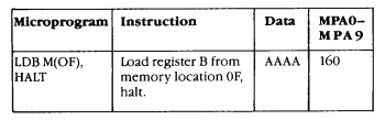 Option Switch Setting:
| 8 | 7 | 6 | 5 | 4 | 3 | 2 | 1 |
| ON | ON | ON | OFF | OFF | OFF | OFF | ON |
This test is similar to Test 10 except that register B is loaded instead of register A.
Test 12
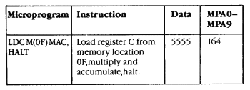 Option Switch Setting:
| 8 | 7 | 6 | 5 | 4 | 3 | 2 | 1 |
| ON | ON | ON | OFF | OFF | OFF | ON | OFF |
This test is similar to Test 10 except that register C is loaded instead of register A.
Loading register C will also start the multiplier/accumulator clock which will produce 33 clock pulses at pin 6 and 8 of the gates at location 8C. During this time, the MACFLAG signal will stall the matrix processor clock so that no strobes will be produced on the WP line until the multiply is finished (about 2.7 microseconds). If the multiplier/accumulator clock was malfunctioning, the matrix processor clock could wait indefinitely and cause the BAD MATH READY LINE message to appear on the Mathbox Tests display in the Self-Test Mode.
The halt command will be generated at the same time as the load C command which causes the MATH RUN line to go low. However, the multiplier/accumulator will continue to operate.
Test 13
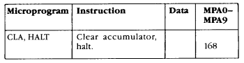 Option Switch Setting:
| 8 | 7 | 6 | 5 | 4 | 3 | 2 | 1 |
| ON | ON | ON | OFF | OFF | OFF | ON | ON |
This test is similar to Test 10 except that the accumulator is cleared instead of loading register A.
Test 14
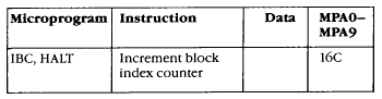 Option Switch Setting:
| 8 | 7 | 6 | 5 | 4 | 3 | 2 | 1 |
| ON | ON | ON | OFF | OFF | ON | OFF | OFF |
This test is similar to Test 10 except that the block index counter is incremented instead of loading register A.
Test 15
 Option Switch Setting:
| 8 | 7 | 6 | 5 | 4 | 3 | 2 | 1 |
| ON | ON | ON | OFF | OFF | ON | OFF | ON |
Test 15 performs the following operations:
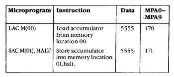
- The 68B09E microprocessor on the Main PCB writes a 170 into the matrix processor address counter during MWO which forms the address for the instruction PROM and is the starting address of the microprogram to be executed. MWO also sets the flip-flop at location 8H in the matrix processor clock which causes the MATH RUN line to go high. A high on the MATH RUN line indicates that the matrix processor is busy, and will stay high until either a HALT command is encountered in the microcode or the microprocessor interrupts the matrix processor. The MATH RUN line is the line actually being checked in the Mathbox Tests self-test. The MATH RUN line allows the matrix processor clock to run and generates the strobes which synchronize the fetching of the micro-instructions. The matrix processor clock produces an instruction cycle time of 416 nanoseconds except when a multiply is being done; then it will wait the 2.7 microseconds required to perform the multiply. (This test does not use the multiplier.)
- The first instruction at address 170 in the instruction PROM will cause register A to be loaded from data memory location 00F, and will also halt the matrix processor. The 16-bit word at instruction PROM location 170 is 848F which functions as follows:
| IP15-0 | Register A Load (Control) |
| IP14-0 | Register B Load (Control) |
| IP13-0 | Register C Load (Control) and Multiply/- |
| | Accumulate |
| IP12-0 | Clear Accumulator (Control) |
| IPll-0 | Increment Block Index Counter (Control) |
| IP10-0 | Halt Matrix Processor (Control) |
| IP9-0 | Road Accumulator (Control) |
| IP8-1 | Load Accumulator (Control) |
| IP7-1 | Address Mode (Control) 1 = Direct |
| IP6-0 | To Matrix Processor RAM Address Bit 6 |
| | through Matrix Processor Address |
| | Selector |
| IP5-0 | To Matrix Processor RAM Address Bit 5 |
| | through Matrix Processor Address |
| | Selector |
| IP4-0 | To Matrix Processor RAM Address Bit 4 |
| | through Matrix Processor Address |
| | Selector |
| IP3-0 | To Matrix Processor RAM Address Bit 3 |
| | through Matrix Processor Address |
| | Selector |
| IP2-0 | To Matrix Processor RAM Address Bit 2 |
| | through Matrix Processor Address |
| | Selector |
| IP1-0 | To Matrix Processor RAM Address Bit 1 |
| | through Matrix Processor Address |
| | Selector |
| IP0-0 | To Matrix Processor RAM Address Bit 0 |
| | through Matrix Processor Address |
| | Selector |
When IP7 = 1, the matrix processor address selector connects IP0-IP6 to MAo-MA6 (the matrix processor RAM address). Address bits MA7-MA10 are set to zero. Thus, the instruction PROM can directly address the first 128 words in the RAM. All of the test programs in the Hardware Diagnostic Tests use this direct address mode.
When IP7 = 0, the matrix processor address selector connects IP0 to MAO and IP1 to MAT. Address bits MA2-MA9 are connected to the block index counter (which is loaded by the microprocessor on the Main PCB). In this addressing mode (the indirect mode) the instruction PROM selects one of the four words in the block selected by the block index counter.
The data at matrix processor RAM location 00F should be 5555. The data was put there by the microprocessor which also has access to the matrix processor RAM.
The one (1) next to Load Accumulator means the accumulator will be loaded with data. The data to be loaded into the accumulator will come from the matrix processor RAM location 000.
The zeros (0) next to the other commands mean that they will not be executed.
IP8 (load accumulator) is actually executed by strobing the outputs of the instruction PROM strobe gates with the WP line. The complement of WP (WP) is used to increment the matrix processor address counter to 171.
- The matrix address counter is now at address 171. The microcode at that location causes the data in the accumulator (previously loaded with 5555) to be written into matrix processor RAM location 001. This instruction is strobed by a special (longer) pulse than the WP At the same time a HALT command is generated, strobed by WP WP increments the matrix processor address counter to 172, which is ignored because the microprogram has finished executing.
Test 16
 Option Switch Setting:
| 8 | 7 | 6 | 5 | 4 | 3 | 2 | 1 |
| ON | ON | ON | OFF | OFF | ON | ON | OFF |
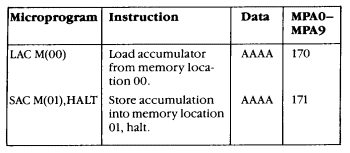
This test is similar to Test 15 except the data is AAAA.
Test 17
 Option Switch Setting:
| 8 | 7 | 6 | 5 | 4 | 3 | 2 | 1 |
| ON | ON | ON | OFF | OFF | ON | ON | ON |
Performs (5555-0000) x 4000 = 5555
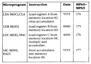
Test 17 performs the following operations:
- The 68B09E microprocessor on the Main PCB writes a 174 into the matrix processor address counter during MWO which forms the address for the instruction PROM and is the starting address of the microprogram to be executed. MWO also sets the flip-flop at location 8H in the matrix processor clock, which causes the MATH RUN line to go high. A high on the MATH RUN line indicates that the matrix processor is busy, and will stay high until either a HALT command is encountered in the microcode or the microprocessor interrupts the matrix processor. The MATH RUN line is the line actually being checked in the Mathbox Tests self-test. The MATH RUN line allows the matrix processor clock to run and generates the strobes which synchronize the fetching of the micro-instructions. The matrix processor clock produces an instruction cycle time of 416 nanoseconds except when a multiply is being done; then it will wait the 2.7 microseconds required to perform the multiply.
- The first instruction at address 174 in the instruction PROM will load register A from data memory location 0C and clear the accumulator at the same time. These instructions are actually executed by strobing the outputs of the instruction PROM strobe gates with the WP line. The complement of the WP line (WP) is used to increment the matrix processor address counter to 175.
- The matrix processor address counter is now at address 175. The microcode at that location will cause register B to be loaded from data memory location OD at the next WP strobe. The matrix processor address counter is incremented to 176.
- The matrix processor address counter is now at address 176. The microcode at that location causes register C (serial multiplier) to be loaded from data memory location 0E at the next WP strobe. The matrix processor address counter is incremented to 177.
Loading register C will also start the multiplier/accumulator clock which will produce 33 clock pulses at pin 6 and 8 of the gates at location 8C. During this time, the MACFLAG signal will stall the matrix processor clock so that no strobes will be produced on the WP line until the multiply is finished (about 2.7 microseconds). If the multiplier/accumulator clock was malfunctioning, the matrix processor clock could wait indefinitely and cause the BAD MATH READY LINE message to appear on the Mathbox Tests display in the Self-Test Mode.
- The matrix processor address counter is now at address 177. The microcode at that location will cause the data from the accumulator to be stored into data memory address 00 (using a special strobe) and will generate a HALT instruction at the end of WP. Thus, the matrix processor clock will stop and the MATH RUN line will go low to indicate that the microprogram has finished executing. The matrix processor address counter will then be incremented to 178, which is ignored.
 Test 18
Option Switch Setting:
| 8 | 7 | 6 | 5 | 4 | 3 | 2 | 1 |
| ON | ON | ON | OFF | ON | OFF | OFF | OFF |
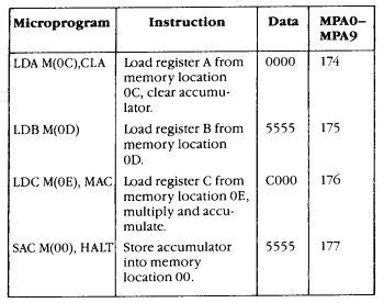
Performs (0000-5555) x 0000 = 5555
This test is similar to Test 17 except the data is different.
Test 19
Option Switch Setting:
| 8 | 7 | 6 | 5 | 4 | 3 | 2 | 1 |
| ON | ON | ON | OFF | ON | OFF | OFF | ON |
Performs (2AAA-0000) x 4000 = 2AAA
This test is similar to Test 17 except the data is different.
Test 20
 Option Switch Setting:
| 8 | 7 | 6 | 5 | 4 | 3 | 2 | 1 |
| ON | ON | ON | OFF | ON | OFF | ON | OFF |
Performs (0000-2AAA) x C000 = 2AAA
This test is similar to Test 17 except that the data is different.
The Mathbox Tests self-test as described in Chapter 2 in the Operators Manual, performs Hardware Diagnostic Test 15 through 20. The Mathbox Tests display will show the option switch setting of any test that fails to produce the correct results.
The first Mathbox Tests self-test performed is similar to Hardware Diagnostic Test 17 without the data shown in the previous table. This test determines whether the math ready line is functioning properly. If not, the message BAD MATH READY LINE will appear on the Mathbox Tests display and the test will remain in a loop. (The other tests will not be run.)
If the math ready line is faulty and stuck low, the result will be some video without enemy ships or stars. If the math ready line is faulty and stuck high, the screen will be completely blank in game mode, but will function during SelfTest.
The Mathbox Tests self-test will also run the following additional tests which cannot be run from the Diagnostic Mode, but can give useful information about a malfunctioning PCB. If one of these tests fails, the letter of the test will be displayed along with the data that failed.
A. Accumulator Test
If the Accumulator Test fails, but Hardware Diagnostic Test 15 through 20 are satisfactory, the problem is likely to be with the shift registers at locations 9A and 9B, or the quad serial adder/subtractor at location 8B (all on the Main PCB).
- Clears the accumulator.
- Performs ACC= 0000 + (0001-0000) x 4000 (the result is 0001).
- Stores ACC into memory.
- Loads ACC back into register A and performs ACC = 0001 + (0001-0000) x 4000 (the result is 0002).
- Repeats parts 3 and 4 which results in the number in the accumulator doubling each time. The sequence is 0001,0002,0004,0008,0010,0020,0040,0080,0100, 0200, 0400, 0800, 1000, 2000, 4000, 8000. (This is referred to as a "walking ones" test.)
B. Block Index Counter and Matrix Processor Indirect Addressing
The 68B09E microprocessor writes data directly into the RAM and, using the block index counter, runs a matrix processor program which uses the block index counter (in the indirect addressing mode).
C. Accumulator Adder Test
This test checks for a particular bit stream through the accumulator at location 8B on the Main PCB as follows:
- Clears the accumulator.
- Performs ACC = (lB2C-0000) x 4000 + (196A-0000) x 4000 (the result is 3496).
D. Subtractor Test
This test checks for a particular bit stream through the serial subtracter at location 8B on the Main PCB as follows:
- Clears the accumulator.
- Performs ACC = (2696-lB2C) x 4000 (the result is 0B6A).
Divider Tests
The divider circuit on the Main PCB is an unsigned 15-bit fractional divider which assumes that the dividend (numerator) is less than twice the divisor (denominator). The hardware consists of a dividend latch, a dividend shift register, a divisor inverting latch, an adder, a difference latch, a quotient shift register with tri-state buffer, and a divider control which includes a divide cycle counter. Refer to the detailed block diagram on Sheet 5B to aid in understanding the circuit operation.
The dividend latch is written into by the microprocessor and has two parts: the dividend latch high byte (DVDDH) and the dividend latch low byte (DVDDL). The dividend latch is not altered by the operation of the divider so it may be left at its previous value, if desired.
The divisor latch is also written into by the microprocessor and has two parts: the divisor high byte (DVSRH) and the divisor low byte (DVSRL). The DVSRH line loads the divisor high byte, clears the quotient shift register, and loads the dividend shift register from the dividend latch. The DVSRL line loads the divisor low byte and starts the divider.
The divider subtracts the divisor from the dividend in the dividend shift register and puts the result in the difference latch. If the result of this subtraction is positive, the carry (C16*) will be a "1." The "1" is shifted into the quotient shift register, and the value from the difference latch is stored into the dividend shift register. (In a conventional divider algorithm, the dividend shift register would then be shifted to the left, but here the output of the adder is wired to the difference latch which is already shifted to the left.) If the result of the subtraction is negative, the carry (C16*) will be a "0." The "0" is shifted into the quotient shift register and the dividend shift register shifts once to the left. The value in the difference latch is otherwise ignored.
The following Test 21 through 25 determines the condition of the divider circuit. The test number will be shown on the display (assuming that the display and the AVG PCB are working). Each test is retriggered every 50 to 60 microseconds for as long as the test is selected.
Perform the Preliminary Procedure under Hardware Diagnostic Tests and set the option switch at location 10D on the Main PCB as indicated in the test.
The Mathbox Tests self-test display performs Hardware Diagnostic Test 21 through 25. The Mathbox Tests display shows the Option switch setting of any test that fails to produce the correct results.
Test 21
Tests for 15 pulses at pin 10 of divide cycle counter at location 8P.
Option Switch Setting:
| 8 | 7 | 6 | 5 | 4 | 3 | 2 | 1 |
| ON | ON | ON | ON | OFF | OFF | OFF | OFF |
4000 (Dividend)/4000(Divisor) = 4000 (Quotient)
Test 22
Tests for shorted bits in the dividend and/or quotient.
Option Switch Setting:
| 8 | 7 | 6 | 5 | 4 | 3 | 2 | 1 |
| ON | ON | ON | ON | OFF | OFF | OFF | ON |
5555 (Dividend)/4000(Divisor) = 5555 (Quotient)
Test 23
Tests for shorted bits in the dividend and/or quotient.
Option Switch Setting:
| 8 | 7 | 6 | 5 | 4 | 3 | 2 | 1 |
| ON | ON | ON | ON | OFF | OFF | ON | OFF |
2AAA (Dividend)/4000(Divisor) = 2AAA (Quotient)
Test 24
Tests for shorter bits in the divisor. The data is inverted and appears at the outputs of the divisor inverting latch at location 4P, 5P, 6P, and 6L.
Option Switch Setting:
| 8 | 7 | 6 | 5 | 4 | 3 | 2 | 1 |
| ON | ON | ON | ON | OFF | OFF | ON | ON |
2AAA (Dividend)/2AAA(Divisor) = 4000 (Quotient)
Test 25
Tests for shorter bits in the divisor. The data is inverted and appears at the outputs of the divisor inverting latch at location 4P, 5P, 6P, and 6L.
Option Switch Setting:
| 8 | 7 | 6 | 5 | 4 | 3 | 2 | 1 |
| ON | ON | ON | ON | OFF | ON | OFF | OFF |
5555 (Dividend)/5555(Divisor) = 4000 (Quotient)
Sound PCB Communications Test
The following Test 26 determines whether the Main PCB can communicate with the Sound PCB. The Main PCB sends a sequence of bytes (5A, 01, 02, 04, 08, 10, 20, 40, and 80) to the Sound PCB that the Sound PCB should echo back. The sequence is repeated as long as the test is selected. If successful, LED 3 will turn on and off about once per second. LED 1 and LED 2 must remain off.
This test does not determine that the Sound PCB is completely functional; only that enough of it is working to communicate with the Main PCB.
Perform the Preliminary Procedure under Hardware Diagnostic Tests and set the option switch at location 10D on the Main PCB as follows:
Test 26
Option Switch Setting:
| 8 | 7 | 6 | 5 | 4 | 3 | 2 | 1 |
| ON | ON | ON | ON | ON | OFF | OFF | OFF |
Troubleshooting With the CAT Box
Troubleshooting the Main PCB
CAT Box Preliminary Set-Up
- Turn off the electrical power to the game.
- Remove the wiring harness from the Electromagnetic Interference (EMI) Shield PCB.
- Disengage the fasteners holding the EMI Shield PCB to the EMI cage by pulling the pins out a short distance.
- Remove the game PCB assemblies from the cage.
- Connect the harness from the game to the EMI Shield PCB edge connectors.
- Connect the WDDIS test point to ground.
- There are two ways that the CAT Box can be connected to the Main PCB:
- Plug the CAT Box Interface cable into the 6809E CAT Box Adapter. Remove the microprocessor from its socket at location 1C on the Main PCB. Plug the 6809E CAT Box Adapter into the empty microprocessor socket at location 1C.
- If you do not have the 6809E CAT Box Adapter, plug the CAT Box interface cable directly into the Main PCB edge connector. This puts the 68B09E microprocessor on the Main PCB in the HALT mode, which puts the address, data, and R/W lines into the high-impedance state and makes it unnecessary to remove the microprocessor from the socket, unless desired.
- Apply power to the game and to the CAT Box.
- Set the CAT Box switches as follows:
- TESTER SELF-TEST: OFF
- TESTER MODE: R/W
- Press TESTER RESET.
Troubleshooting the Address Lines
- Perform the CAT Box Preliminary Set-Up procedure under Troubleshooting the Main PCB.
- Connect the Data Probe to the CAT Box.
- Connect the Data Probe ground clip to a ground test point on the Main PCB.
- Set the CAT Box switches as follows:
- BYTES: 1
- PULSE MODE: UNLATCHED
- R/W MODE: (OFF)
- R/W: WRITE
- Key in the address pattern given in Table 4 with the CAT Box keyboard (use AAAA to start)
- Press DATA SET.
- Key in AA with the keyboard.
- Set R/W MODE to STATIC.
- Probe the IC-pins listed in Table 4 with the DATA PROBE and check that the corresponding 1 or 0 LED on the CAT Box lights up.
- Repeat parts 4c through 9 using address 5555 in part and data 55 in part 7.
Troubleshooting the Data Lines
- Perform the CAT Box Preliminary Set-Up procedure under Troubleshooting the Main PCB.
- Connect the Data Probe to the CAT Box.
- Connect the Data Probe ground clip to a ground test point on the Main PCB.
- Set the CAT Box switches as follows:
- BYTES: 1
- R/W MODE: (OFF)
- R/W: WRITE
- Key in address 0000 with the keyboard.
- Press DATA SET.
- Key in data AA with the keyboard.
- Set R/W MODE to PULSE and then to STATIC.
- Probe the IC-pin listed in Table 5 with the DATA PROBE and check that the 1 or 0 LED on the CAT Box lights up.
Troubleshooting the Program RAM
- Perform the CAT Box Preliminary Set-Up procedure under Troubleshooting the Main PCB.
- Set the CAT Box switches as follows:
- DBUS SOURCE: ADDR
- BYTES: 1024
- R/W MODE: (OFF)
- R/W: WRITE
- Enter address 4800 with the keyboard.
- Set R/W MODE to PULSE and back to (OFF).
- Set R/W to READ.
- Set R/W MODE to PULSE and back to (OFF)
- The Program RAM is a 2K x 8 device. To test the entire device perform parts 2 through 6 with the address in part 3 at 4C00.
- If the CAT Box reads an address that does not match that entered with the CAT Box keyboard, the COMPARE ERROR LED will light up.
Troubleshooting with Checksums
- NOTE - This procedure can only be done with those CAT Boxes equipped with a Checksum switch.
- Perform the CAT Box Preliminary Set-Up procedure under Troubleshooting the Main PCB.
- Set the CAT Box switches as follows:
- BYTES: 1024
- DBUS SOURCE: DATA
- R/W MODE: (OFF)
- CHECKSUM SWITCH: ON
- Key in the address pattern given in Table 6.
- Set the R/W MODE switch to PULSE and then back to (OFF).
- Check the CAT Box ADDRESS/SIGNATURE display for the appropriate checksum.
- Repeat parts 3 through 5 for each address listed in table 6.
1MPAGE must be low. If not, ground the RESET test point on the Main PCB.
2'MPAGE must be high. If not, use the CAT Box to write 80 (data) to 4684 (address).
3All of the Self-Test and Hardware Diagnostics Tests are in this ROM.
Troubleshooting the Option Switch Inputs
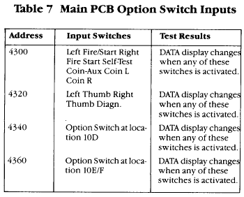
- Perform the CAT Box Preliminary Set-Up procedure under Troubleshooting the Main PCB.
- Set the CAT Box switches as follows:
- Set the CAT Box as follows for each address listed in Table 7:
- Set R/W MODE to (OFF).
- Enter the address with the keyboard.
- Set R/W MODE to STATIC.
- Activate the input switch indicated in Table 4 for the address.
If the preceding procedures for troubleshooting the Main PCB are successful, then there should be enough of the game microprocessor system working to perform the SelfTest and Hardware Diagnostic Tests procedures.
Troubleshooting the Sound PCB
CAT Box Preliminary Set-Up
- Turn off the electrical power to the game.
- Remove the wiring harness from the EMI Shield PCB.
- Disengage the fasteners holding the EMI Shield PCB to the EMI cage by pulling the pins out a short distance.
- Remove the game PCB assemblies from the cage.
- Connect the harness from the game to the EMI Shield PCB edge connectors.
- Connect the WDDIS test point to ground. Plug the CAT Box Interface cable into the 6809E CAT Box Adapter.
- Remove the microprocessor from its socket at location 3K on the Main PCB and plug the 6809E CAT Box Adapter into the empty socket at location 3K.
- Apply power to the game and to the CAT Box.
- Set the CAT Box switches as follows:
- TESTER SELF-TEST: OFF
- TESTER MODE: R/W
- Press TESTER RESET.
Troubleshooting the Address Lines
- Perform the CAT Box Preliminary Set-Up procedure under Troubleshooting the Sound PCB.
- Connect the Data Probe to the CAT Box.
- Connect the Data Probe ground clip to a ground test point on the Sound PCB.
- Set the CAT Box switches as follows:
- BYTES: 1
- PULSE MODE: UNLATCHED
- R/W MODE: (OFF)
- R/W: WRITE
- Key in the address pattern given in Table 8 with the CAT Box keyboard (use AAAA to start).
- Press DATA SET.
- Key in AA with the keyboard.
- Set R/W MODE to STATIC.
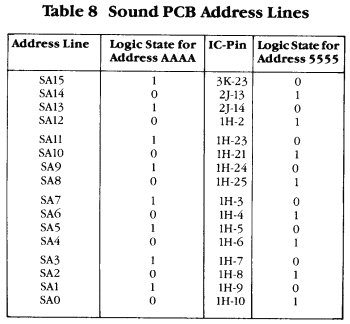
- Probe the IC-pin listed in Table 8 with the Data Probe and check that the corresponding 1 or 0 LED on the CAT Box lights up.
- Repeat parts 4C through 9 using address 5555 in part 5 and data 55 in part 7.
Troubleshooting the Data Lines
- Perform the CAT Box Preliminary Set-Up procedure under Troubleshooting the Sound PCB.
- Connect the Data Probe to the CAT Box.
- Connect the Data Probe ground clip to a ground test point on the Sound PCB.
- Set the CAT Box switches as follows:
- BYTES: 1
- R/W MODE: (OFF)
- R/W: WRITE
- Key in address 0000 with the keyboard.
- Press DATA SET.
- Key in data AA with the keyboard.
- Set R/W MODE to PULSE and then to STATIC.
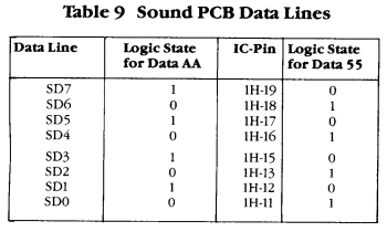
- Probe the IC-pin listed in Table 9 with the Data Probe and check that the corresponding 1 or 0 LED on the CAT Box lights up.
Troubleshooting the Program RAM
- Perform the CAT Box Preliminary Set-Up procedure under Troubleshooting the Sound PCB.
- Set the CAT Box switches as follows:
- DBUS SOURCE: ADDR
- BYTES: 1024
- R/W MODE: (OFF)
- R/W: WRITE
- Enter address 2000 with the keyboard.
- Set R/W MODE to PULSE and back to (OFF).
- Set R/W to READ.
- Set R/W MODE to PULSE and back to (OFF).
- The program RAM is a 2K x 8 device. To test the entire device, perform parts 2 through 6 with the address in part 3 at 2400. There is also 128 bytes of RAM in the 6532, starting at 1000.
- If the CAT Box reads an address that doesn't match that entered with the CAT Box keyboard, the COMPARE ERROR LED will light.
Troubleshooting with Checksums
- NOTE - This procedure can only be done with those CAT Boxes equipped with a Checksum switch.
- Perform the CAT Box Preliminary Set-Up procedure under Troubleshooting the Sound PCB.
- Set the CAT Box switches as follows:
- BYTES: 1024
- DBUS SOURCE: DATA
- R/W MODE: (OFF)
- CHECKSUM SWITCH: ON

- Key in the address pattern given in Table 10.
- Set the R/W MODE switch to PULSE and then back to (OFF).
- Check the CAT Box ADDRESS/SIGNATURE display for the appropriate checksum.
- Repeat parts 3 through 5 for each address listed in Table 10.
Analog Vector-Generator Signature Analysis
The following procedure initializes the vector RAM and prevents resets. During signature analysis the normal execution of vector instructions is changed so that the vector address controller increments the vector address after every cycle. Vector HALT instructions are also ignored.
The state machine feedback is disconnected and instead the state machine PROM is driven by the vector address bus. This causes the state machine PROM to cycle sequentially through its addresses rather than be dependent upon the particular vector instruction being executed. In this way, the data from the vector memory does not affect the signatures generated by the state machine so that malfunctioning circuits can be easily located.
- Set the Self-Test switch to the on position.
- Ground the DIAGN test point on the Main PCB.
- Set the option switch at location 10D on the Main PCB as follows:
| 8 | 7 | 6 | 5 | 4 | 3 | 2 | 1 |
| ON | ON | OFF | OFF | OFF | ON | ON | OFF |
- Perform the CAT Box Preliminary Set-Up procedure under Troubleshooting the Sound PCB.
- Connect the CAT Box Signature Analysis ground to the AVG PCB ground.
- Connect the CAT Box Signature Analysis START and STOP to VRAM I at pin 2 of the vector address decoder at location 2K on the AVG PCB.
- Connect the CAT Box Signature Analysis CLOCK to the SACLK test point on the AVG PCB.
- Set the Signature Analyzer as follows:
- START: negative
- STOP: positive
- CLOCK: negative
- Ground the test point marked SA on the AVG PCB.
- Momentarily ground the RESET test point on the Main PCB.
- Compare signatures to those shown on the AVG PCB schematics.
- NOTE - If the vector RAM loses its data during signature analysis (due to the Data Probe shorting together two or more leads), momentarily ground the RESET test point on the Main PCB.
Remember, the FORCE will be with you -- ALWAYS!
HTML'ized version of this is Copyright © 1997 Jess Askey